
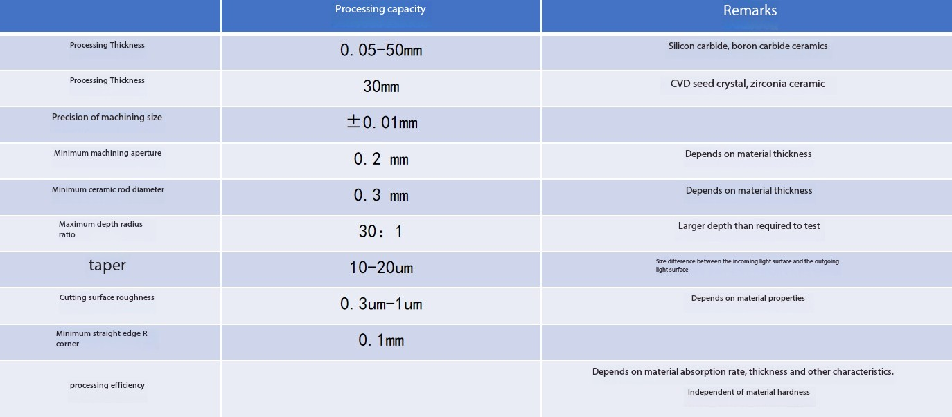
Processing Thickness: 0.05-50mm (Silicon Carbide, Boron Carbide Ceramics)
Processing Thickness: 30mm (CVD Seed, Zirconia Ceramics)
Processing Dimensional Accuracy: ±0.01mm
Minimum Processing Aperture: 0.2 mm (related to material thickness)
Minimum Ceramic Rod Diameter: 0.3 mm (related to material thickness)
Maximum Depth-to-Diameter Ratio: 30:1 (larger ratios require testing)
Taper: 10-20um (size difference between light-incident surface and light-emergent surface)
Cut Surface Roughness: 0.3um-1um (related to the material itself)
Minimum Straight Edge R Angle: 0.1mm
Processing Efficiency: Related to characteristics such as material light absorption rate and material thickness. Not related to material hardness.
Our product center maintains a steadfast focus on innovation and has secured hundreds of technological patents.
9AM - 5:30PM
Our Office Hours: Mon. - Fri.
TEL:+86 18723607109
EMAIL:Server@sovix.cn
ADD:ChongQing China